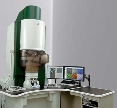
 March 18, 2010, Peabody, Mass. — JEOL USA and the University of Texas at Dallas (UTD) today jointly announced the University’s acquisition of the new JEOL atomic resolution Transmission Electron Microscope (TEM). The new ARM200F is an aberration-corrected TEM that achieves better than 1 Angstrom resolution in STEM and TEM and chemical analysis at the atomic level.
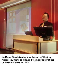
The announcement was made during a JEOL USA “Nano and Beyond” electron microscopy seminar held in the University’s Natural Science and Engineering Research Laboratory. Dr. Moon Kim, Professor of Materials Science and Engineering, hosted the seminar attendees during a tour of the future site of the new TEM, the Nano and Beyond Microscopy Lab, of which he is the Director.
With the acquisition of the ARM200F TEM, UT Dallas will advance its role as key contributor to the development of next-generation semiconductor devices and as a resource for local industry research and that of several technical consortiums.
“This is a great opportunity to further enhance the University’s impact on the future development of semiconductor technology and re-energize nano research in this area,” Dr. Kim said. UTD is a hub for two semiconductor research consortiums, infusing the area with new business opportunities: the Texas Fusion (Future Semiconductor Commercialization) consortium, financed by the South Korean government and the Texas Emerging Technology Fund, and the Silicon Wafer Engineering and Defect Science Industry/University Cooperative Research Center (SiWEDS IU/CRC), an independent center supported by the University and corporate members. UTD is also a p art of the Southwest Academy of Nanoelectronics (SWAN), a nationally funded research center. Kim’s Nano and Beyond lab has a staff of 14 members and is home to two field emission JEOL TEMs.
Nanotechnology research with the advanced capabilities of the new TEM will offer greater insight into atomic structures of device materials, allowing researchers to develop smaller and more efficient semiconductor chips, and explore novel nanomaterials for new semiconductor devices.
Dr. Kim anticipates that the availability of next-generation electron microscope technology will also be a major draw for materials researchers as well as fledgling tech firms producing peripheral imaging equipment.
JEOL USA introduced the ARM200F, a totally new TEM design from the ground up, with extraordinary stability and picometer resolution, in 2009. “We look forward to collaborating with Moon Kim and UT Dallas in advancing nanotech research with this new TEM. We’re excited that we can participate in future projects using never-before-seen imaging resolution and chemical spatial resolution – all at acquisition speeds never before possible,” said Dr. Thomas Isabell, JEOL USA TEM Product Director.
https://www.jeolusa.com/NEWS-EVENTS/Press-Releases/PostId/93/UT-Dallas-Re-energizes-Semiconductor-Nano-Research-with-Acquisition-of-New-JEOL-Atomic-Resolution-Microscope


