Researchers use helium ion microscopy to engineer atomic defects in molybdenum disulfide (MoS2)
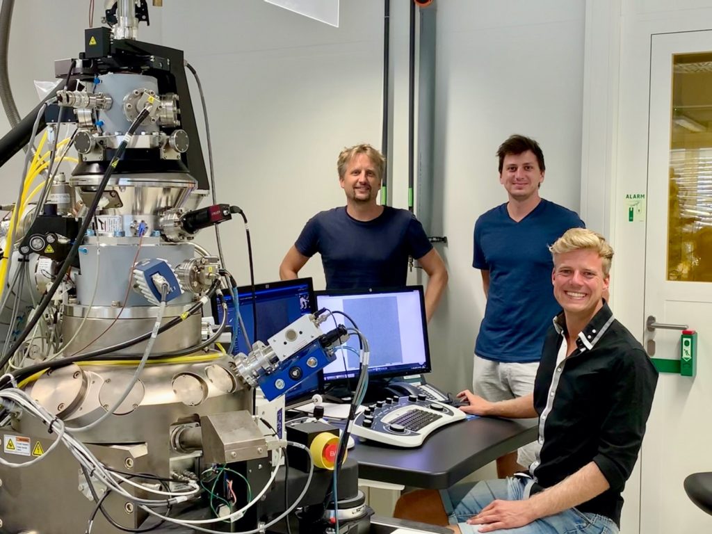
Prof. Alexander Holleitner, Dr. Christoph Kastl, and Elmar Mitterreiter, who performed the HIM-lithography at the atomistic limit.
Prof. Alexander Holleitner and his group head the Center of Nanotechnology and Nanomaterials of the Walter Schottky Institute (WSI) of TUM. As the name implies, they work with materials on the nanometer scale, e.g. two-dimensional semiconductors and topological quantum materials. They want to fully exploit the potential of nanoscale circuits for optoelectronic and photovoltaic applications, as well as for communication and information technologies. For this, their facilities are specialized on research on nanometer scale structures with manipulation and investigation of materials on the atomic scale.
In a set of recent publications in Nature Communications and Nano Letters, a WSI-team lead by Prof. Holleitner and Prof. Finley used helium ion microscopy to engineer atomic defects in two-dimensional materials, such as the semiconducting molybdenum disulfide (MoS2). We interviewed Prof. Holleitner and Elmar Mitterreiter, a member of his team and co-author on the publications, about their work.
What research questions did you ask that led you to perform this work?
Quantum technology is gaining in importance. Intense research is done regarding the realization of the smallest building blocks for information technologies and the right host materials for possible quantum technologies. To realize industrial applications, one requires a scalable, fast, and highly precise nano-patterning technique for creation of the smallest functional units in the right material. Two-dimensional materials combine unique electronic and optical properties with a natural out-of-plane confinement on the atomic scale and are ideal candidates as host materials. We asked ourselves how we can implement functionalities on an atom scale in 2D materials, such as MoS2. For instance, how precisely can atomistic, yet optically active defects be fabricated in large scale applications? What are the exact physical processes during fabrication and usage?
How does the Helium Ion Microscope (HIM) enable this type of work?
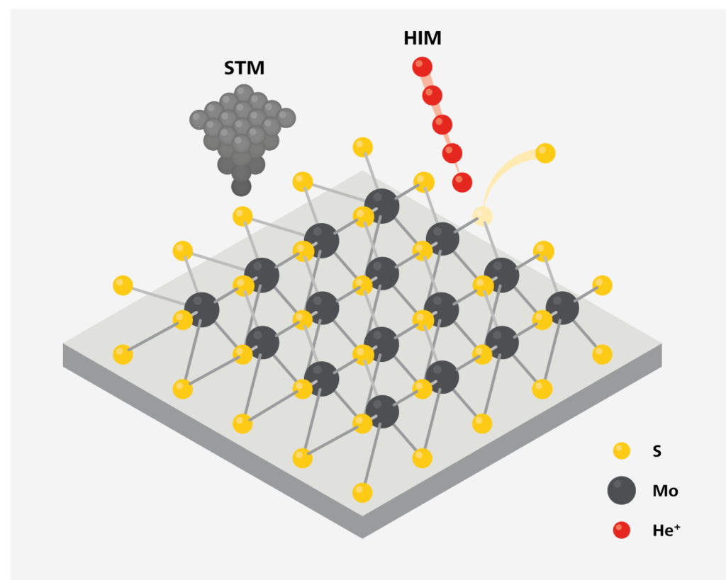
High-resolution patterning of 2D materials using helium ion microscopy (HIM). Schematic representation of single-layer molybdenum disulfide under helium ion irradiation (red) and the subsequent investigation using scanning tunneling microscopy (STM).
Due to the two-dimensional nature of the studied host materials, a highly surface sensitive nano structuring technique is required. Furthermore, high precision, scalability, and high patterning speed are needed for potential industrial applications.
The Helium Ion Microscope (HIM) combines all required properties. For the studied materials, the interaction cross section of the He-ions and the MoS2 combined with the sub-nanometer He-ion beam enable highly precise removal of single atoms in the MoS2 host crystal.
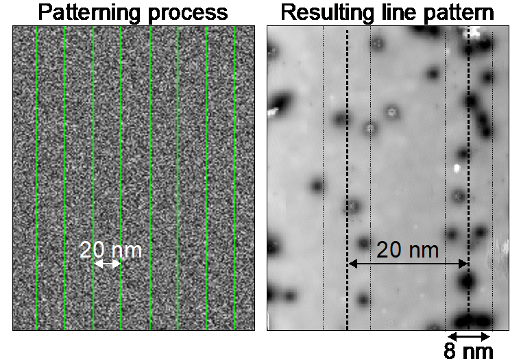
Patterning process using helium ion microscopy. Left: Green lines represent the desired line-shape pattern with a pitch of 20 nm. Right: Resulting line-shape in single-layer molybdenum disulfide resolved with a scanning tunneling microscope (STM). The distance between the lines occurs to be 20 nm (as desired). However, we find an average width of approximately 8 nm of each line. STM-measurements performed at the Molecular Foundry (Berkeley, USA) together with Bruno Schuler and Alex Weber-Bargioni.
What were your key findings? Were any of the results surprising or particularly exciting?
The Helium Ion Microscope (HIM) allows us to create several different types of defects with high precision below 10 nanometer in 2D MoS2. By comparing this number to the beam diameter of the incident He-ions (below 1 nanometer) we found out that the precision of the defect creation is mainly limited by backscattered ions from the supporting substrate. We further investigated the defects and identified the most frequently created ones. Apparently, sulfur vacancies act as single photon emitters, the fundamental building blocks for quantum communication and more.
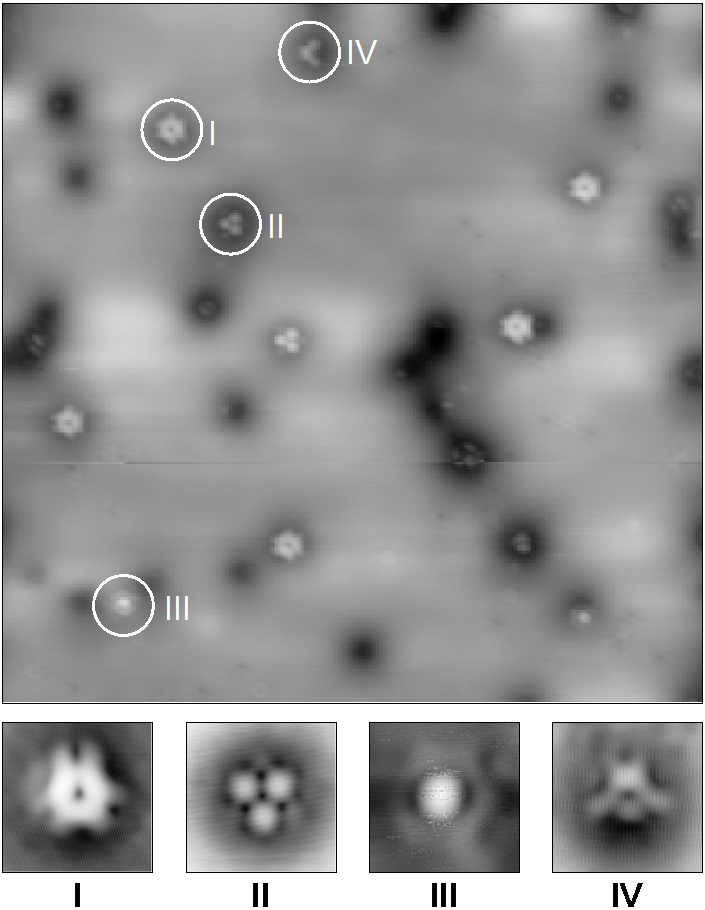
Scanning Tunneling Microscopy (STM) image of molybdenum disulfide irradiated with a constant helium ion dose and measured at the Molecular Foundry (Berkeley, USA) together with Bruno Schuler and Alex Weber-Bargioni. The bombardment induces four types of defects labelled I-IV. Additionally, charged defects appear as black circular features in the image. cf. E. Mitterreiter et al. Nano Letters 2020.
What are potential applications for this work?
The ability to create atomic defects on a large scale with high precision enables several different applications. The mentioned single-photon emission is fundamental for a variety of quantum technological applications. Furthermore, on a larger horizon, we found out that some of the He-ion induced defects are also catalytically active and can be used to split water into hydrogen and oxygen. This process could enable a sustainable and clean energy provision for the future.
In general, the high precision of the Helium Ion Microscopy (HIM) enables research solid state physicists have dreamed about for decades.
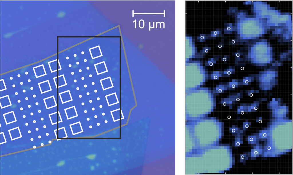
Left: Optical microscopy image of single-layer molybdenum disulfide with desired helium-ion pattern. White squares show regions with constant helium ion dose, the white circles represent individual HIM induced point defects. Right: Photoluminescence map of HIM irradiated area shown by the black rectangle (left). Black areas show no defect luminescence, green and blue areas represent defect luminescence. The position of the defect-related emission perfectly agrees with the spatial position of the helium ion induced defects. Measurements provided by K. Barthelmi and L. Sigl (TUM).
Where do you see your research going next?
In the next steps, we try to gain more understanding of the He-ion fabricated single photon emitters. We need to fully understand the exact physical processes causing the single photon emission to better control them and reach their full potential in quantum technological applications, for example by using the entanglement of photon pairs for communication protocols. We are only at the beginning of the so-called second quantum revolution and it is still a long way to fully understand and control these quantum phenomena.
Learn More
- Atomistic positioning of defects in helium ion treated single layer MoS2. Nano Letters
- Atomistic defects as single-photon emitters in atomically thin MoS2. APL Perspective
- Scalable single-photon sources in atomically thin MoS2. arXivLabs
- Robust valley polarization of helium ion modified atomically thin MoS2. 2D Materials
- Site-selectively generated photon emitters in monolayer MoS2 via local helium ion irradiation. Nature Communications
Get information on ZEISS helium ion microscopy.


