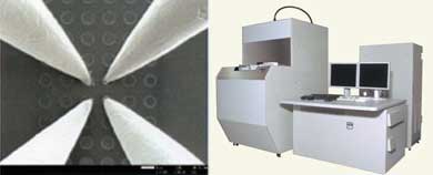
February 13, 2007, Peabody, MA – The high spatial resolution and flexibility of the JEOL Beam Tracer allows this new failure analysis tool to precisely locate and mark defect sites in multi-layer semiconductor devices. The Beam Tracer images marginal and failed interconnects and junctions through several complex layers. It allows measurement of individual transistors, performs electrical characterization, and includes a patented Voltage Distribution Contrast method for devices produced under the 65nm design rule.

A precision probing system based on SEM technology, the Beam Tracer incorporates four mechanical probes that can be moved in increments of less than 1nm.
The probes detect electron beam absorption current to evaluate electrical characteristics in ICs and identify abnormal resistance in interconnects and contacts.
Using the patented Voltage Distribution Contrast (VDIC) method, the Beam Tracer detects a wide range of multiple marginal failures without repositioning the probes. This flexible tool can detect resistive areas from 100 ohms to infinity.
An e-beam assisted marking tool makes it easy to rapidly locate defects for further analysis using a FIB for TEM analysis.
JEOL will introduce the Beam Tracer at Semicon West, July 17-19, 2007, in San Francisco. Visit JEOL at booth #1105 at the Moscone Center.
For further information, please visit the Beam Tracer product information page.
https://www.jeolusa.com/NEWS-EVENTS/Press-Releases/PostId/48/New-Failure-Analysis-Tool-from-JEOL


