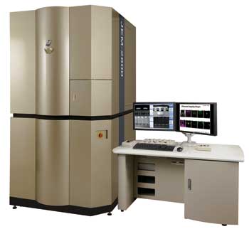
 July 12, 2011 (Peabody, Mass.) — A new 200kV Transmission Electron Microscope from JEOL delivers high throughput nano-analysis for process and quality control of mass produced semiconductor and materials samples. The multi-function JEOL JEM-2800 features high resolution imaging in TEM, STEM, and SE modes; ultrasensitive elemental mapping with a large angle Energy Dispersive Spectrometer (EDS); Electron Energy Loss Spectroscopy (EELS) for chemical analysis; critical dimension analysis; tomography; and in situ observation of samples. The all-new TEM functions without use of the traditional fluorescent screen on the electron column.
The JEM-2800 speeds specimen observation through fully automatic functions including adjustment of focus, astigmatism, contrast, brightness, crystal zone axis alignment, and height. Switching between analysis modes is seamless, and quick data collection shortens turnaround time between samples. An operator navigation system and on-screen operating guide make the JEM-2800 a high throughput, user-friendly TEM for any skill level.
Additional features and key specifications of the JEM-2800 include a Schottky field-emission electron gun, highly stable eucentric side-entry goniometer stage, a magnification range of 100X to 150,000,000X using STEM, 0.1nm TEM resolution and 0.20nm BF/DF STEM resolution.
The JEM-2800 is JEOL’s latest addition to its comprehensive lineup of 100-300kV TEMs and most recently the ARM200F atomic resolution TEM. The first U.S. customer, a global semiconductor manufacturer, will take delivery of the new JEM-2800 with large solid angle EDS this summer.
https://www.jeolusa.com/NEWS-EVENTS/Press-Releases/PostId/114/JEOL-Unveils-New-High-Throughput-Automated-TEM-for-Nano-analysis


