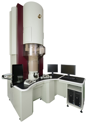
 JEOL Ltd. (President Gon-emon Kurihara) is pleased to announce the development and start of sales of a new atomic resolution electron microscope, JEM-ARM300F.
Product development background
Transmission electron microscopy (TEM) has long been a tool essential for micro structure evaluation in the field of materials development. However, as the fine structures of advanced materials are being designed at the nano level or atomic level, the synthetic process for such materials increasingly requires imaging and analysis at higher resolution.
To meet this demand, JEOL has focused on development of a transmission electron microscope incorporating spherical aberration correctors to exceed the current resolution boundary. In 2009, JEOL announced the JEM-ARM200F, a 200 kV atomic resolution analytical transmission electron microscope featuring spherical aberration correctors, which achieved a resolution of 80 pm (scanning transmission (STEM) image) as the first ever commercial electron microscope. To achieve the atomic level resolution, the JEM-ARM200F incorporates various capabilities to ensure highly stable operation. With over 100 units of the ARM200F currently in operation worldwide, many researchers have become familiar with atomic level imaging and analysis.
Meanwhile, as aberration correctors are widely used, various new requirements for transmission electron microscopy are emerging, in addition to higher resolution, including higher analytical sensitivity, in-situ imaging, flexible accelerating voltage control, and ease of operation for aberration correction.
Thus, JEOL developed the JEM-ARM300F, a 300 kV atomic resolution transmission electron microscope featuring JEOL’s own aberration correctors as an enhanced model of the JEM-ARM200F. Nicknamed GRAND ARM, the JEM-ARM300F, incorporates JEOL’s propriety dodecapole correctors, successfully increasing the resolution level to 63 pm (STEM resolution). The GRAND ARM can be configured for ultra high resolution imaging or analytical applications for high sensitivity and in-situ analysis according to the user’s needs.
The system is primarily intended for public and private research institutes and semiconductor manufacturers.
Main Features
- Ultra high resolution imaging – Achieves a resolution of 63 pm in the scanning transmission electron microscope image (STEM) mode at an accelerating voltage of 300 kV, using JEOL’s own spherical aberration corrector for the illumination system.
- High performance cold-cathode field-emission electron gun featuring high brightness and low energy dispersion – Incorporates a new high performance cold cathode electron gun as standard; the high brightness beam with minimum chromatic aberration allows for high resolution imaging and analysis.
- Wide accelerating voltage range – Supports accelerating voltage levels of 300 kV and 80 kV as standard; other accelerating voltage levels are optionally available as needed.
- Aberration corrector integrated with microscope base unit – Incorporates JEOL’s proprietary spherical aberration correctors in the image forming system (TEM aberration corrector) and in the illumination system (STEM spherical aberration corrector).
- Aberration corrector control system – Uses the JEOL COSMO (JEOL Corrector System Module) system for auto control of the aberration correctors.
- Two types of objective lens pole piece – Two types of objective lens polepiece are available to meet a wide range of users’ applications.
- Vacuum system featuring dry pre-evacuation and high vacuum – The vacuum system features a pre-evacuation system incorporating a turbo molecular pump as standard and an enhanced column evacuation system, achieving higher vacuum while minimizing contamination and damage in atomic level imaging and analysis.
- Stable column/console, specimen stage, and electrical system – The column, 330 mm in diameter, features a higher level of mechanical rigidity. The microscope base unit is also designed to enhance its mechanical/electrical stability and resistance to environment, fully utilizing the stabilizing technologies developed for the JEM-ARM200F.
- A complete line of signal detectors – A complete line of signal detectors are available, including EDS (energy dispersive X-ray spectrometer) up to 100 mm2 and EELS (electron energy loss spectrometer), backscattered electron detectors, and up to 4 STEM detectors. The microscope also supports simultaneous observation of high angle annular dark field image, low angle annular dark field image, annular bright field image, and bright field image.
Main Specifications
| Accelerating voltage | Maximum 300 kV |
| TEM lattice resolution | 0.05 nm (with spherical aberration corrector for image forming system) |
| STEM resolution | 0.063 nm (spherical aberration corrector for illumination system) |
# # #
JEOL USA, Inc.
JEOL is a world leader in electron optical equipment and instrumentation for high-end scientific and industrial research and development. Core product groups include electron microscopes (SEMs and TEMs), instruments for the semiconductor industry (electron beam lithography and a series of defect review and inspection tools), and analytical instruments including mass spectrometers, NMRs and ESRs.
JEOL USA, Inc., is a wholly owned subsidiary of JEOL, Ltd., Japan, was incorporated in the United States in 1962. The company has 13 regional service centers that offer unlimited emergency service and support in the U.S.
For more information about JEOL USA, Inc. or any JEOL products, visit www.jeolusa.com, or call 978-535-5900.
https://www.jeolusa.com/NEWS-EVENTS/Press-Releases/PostId/136/Grand-ARM-Offers-Unprecedented-63pm-Resolution


